Solder Paste Inspection, condensed as SPI, is a specific cycle that assesses/investigates solder paste store quality. It guarantees the right testimony of solder paste on the board without deficiencies. In the majority of the cases, the explanation for the ill-advised working of the PCB is because of inappropriate solder paste printing. Solder paste inspection is subsequently a fundamental method that guarantees costs are kept as low as conceivable by identifying deficiencies in the solder printing phase of the creation line. Solder paste affidavit during a printing interaction is a vital undertaking to append the parts to a circuit board for keeping a legitimate electrical association.
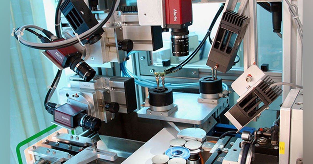
Surface Mount Technology (SMT) inspection process uses both Automated Optical Inspection (AOI) and X-beam to outwardly check the outer layer of the board utilizing top quality (HD) cameras and a few light sources. These frameworks utilize the caught picture and contrast it and the ideal/regular board picture which is as of now saved in the framework. An examination is then made between the caught picture and the best picture to recognize and feature any imperfections or suspected regions.
Automated Optical Inspection (AOI)
AOI machine tests and assesses PCBs for shortcomings like presence or nonattendance, part position deserts, layered imperfections, and surface deformities. With the headway of electronic agreement assembling and circuit intricacy, it has become impractical to physically perform SMT inspection. In this way, AOI assumes a significant part in sheets after PCB get together. The machine has the ability of recognizing blunders in the beginning phase of the assembling system to guarantee the PCB quality prior to moving to the following assembling step.
The AOI machine can examine all size parts, for example, 01005, 0201, and 0402s and bundles like CSPs, BGAs, LGAs, PoPs, and QFNs. At first, AOI machines were intended for 2D estimations/examination (discovery along X and Y organizes as it were). With the expansion of 3D frameworks, the estimation along Z coordinate has likewise become conceivable. A definitive point of an AOI machine is to recognize mistakes in the creation line and quickly illuminating something similar to AOI developers (otherwise called criticism). Input to the AOI developers is both useful and essential so that time could be saved during SMT inspection.
AOI Programmers
The automated optical inspection machine runs on a devoted program, created by AOI software engineers. Coming up next are the circumstances under which criticism is produced:
- Part depictions are absent
- The hunt region should be adjusted
- Part markings should be revised, added, or erased
- SMT Inspection/Bare PCB Inspection
X-Ray Inspection System/Automated X-beam Inspection (AXI)
A PCB X-beam inspection framework, otherwise called automated X-beam Inspection (AXI), utilizes X-beam radiation rather than apparent light to distinguish stowed away PCB deformities,.
The previously mentioned absconds shouldn’t be visible during the inspection by standard cameras or by the unaided eye. X-beam inspection is a generally utilized procedure that can recognize producing abandons. The X-beam inspection machine can examine the PCB from any point.
Structure/Principle of Operation for X-beam Machine
An inspection gadget in light of X-beams comprises of a chamber with a little hole where it is feasible to embed and eliminate the PCB. The X-beam source is normally situated at the lower part of the chamber. Inside the chamber, an advanced finder (phosphor screens) is situated straight over the X-beam source. Utilizing an edge transport line, the PCB that should be inspected enters the chamber and is situated between the source and the finder. The posterior of the PCB is presented to the X-beam with the goal that the X-beam can go through the parts.
While AOI creates full shading pictures of the article surface, X-beam machine sends X-beams through the items and records dim scale pictures of the shadows. The picture handling programming then, at that point, processes the picture. It then, at that point, identifies the area and size/state of anticipated elements (for process improvement) alongside the presence/nonappearance of unfamiliar articles or highlights (for oddity discovery). Check for more here.
Inside the part, the different atomic densities lessen the X-beams by various sums, bringing about the production of light and dull regions in investigator media. Therefore, we can without much of a stretch recognize breaks, for example the lessening level of the thick piece of the solder ball is weighty contrasted with the constriction level of the break or air. The break will in general be dull because of changing weakening levels, and the thick piece of the solder ball shows up as a light in the picture.